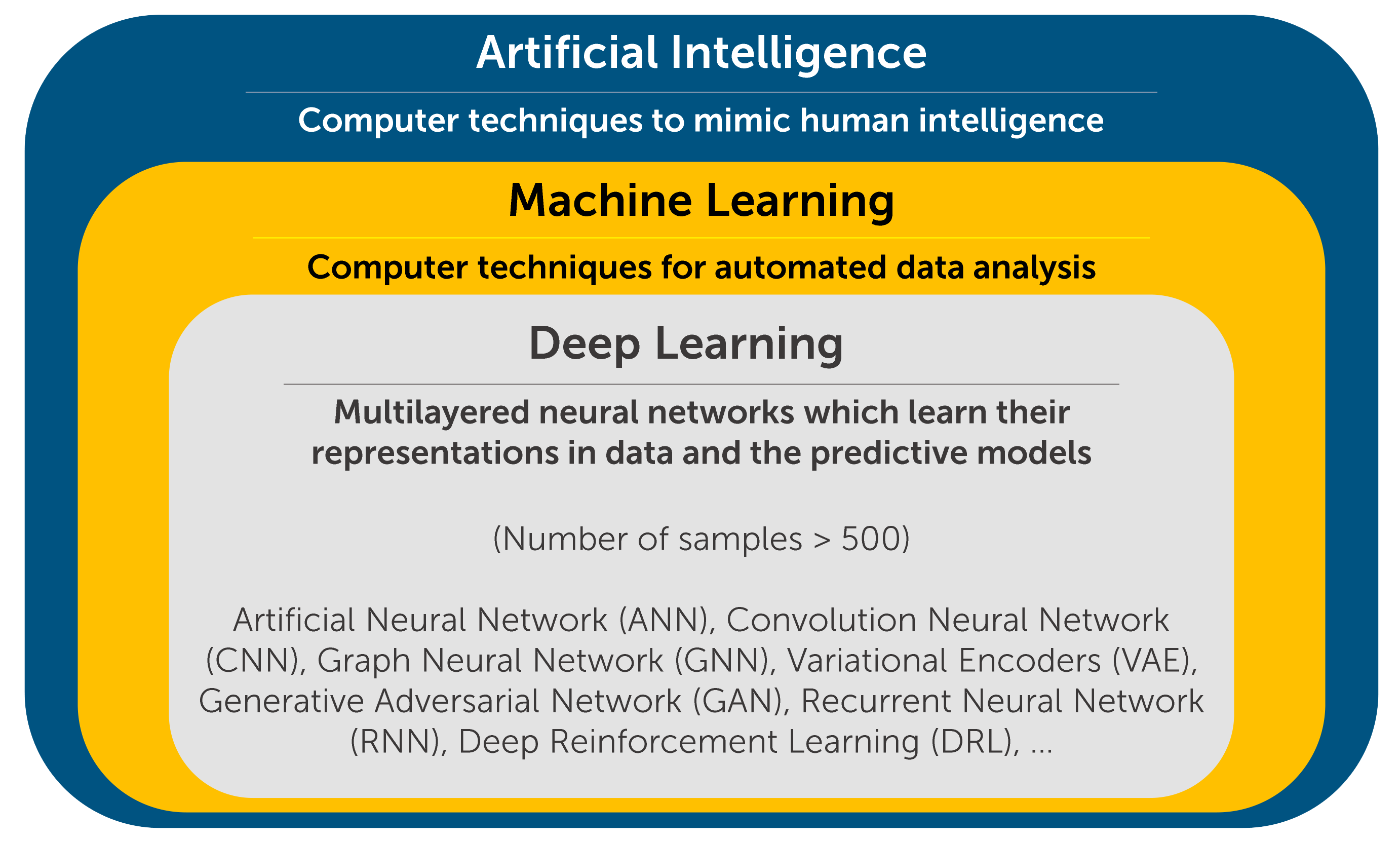
The energy band gap is a crucial parameter in determining the functionalities of a semiconductor in optics, optoelectronics, microelectronics, and photovoltaics applications [1,2]. Consequently, considerable effort has been made to develop theoretical methods for high-throughput calculations of this electronic property. Over the past decades, ab initio simulations have been widely used to calculate the electronic properties of many materials, leading to the creation of large-scale materials data and computational infrastructures [3–8]. These ever-growing data infrastructures provide fertile grounds for the emergence of novel materials modeling by employing data-driven approaches [9–11]. Machine learning (ML) [12] and artificial intelligence [13] have become increasingly popular as efficient machinery for predicting material properties. The most pertinent aspect of every ML model for materials property prediction is properly encoding material information, including chemical composition and atomistic structure [14]. These materials’ representations capture the underlying mechanism of a desired material property and map materials samples to feature spaces amenable to learning approaches. We aim to evaluate the performance and identify the domain of applicability of ML for predicting the band gap of semiconductors and insulators using different classes of structural features. The special significance of our research is its potential to produce a transferable ML model for reliable prediction of the theoretical band gap of semiconductors and insulators. In other words, this model is likely not limited to specific datasets or certain structures. In this regard, we will quest for three central requirements: the best combinations of primary features, the most efficient structural features, and the broadest domain of applicability for ML prediction of the theoretical band gap of materials.
[1] S. Sze et al., Physics of semiconductor devices (John Wiley & Sons, Ltd, 2006).
[2] D. Neamen, Semiconductor physics and devices (McGraw-Hill Higher Education, 2011).
[3] S. P. Huber et al., Sci. Data 7, 1 (2020).
[4] C. Draxl et al., J. Phys. Mater. 2, 036001 (2019).
[5] S. Curtarolo et al., Comp. Mat. Sci. 58, 218 (2012).
[6] L. Talirz et al., Sci. Data 7, 1 (2020).
[7] A. Jain et al., APL Mater. 1, 011002 (2013).
[8] S. Kirklin et al., npj Comput. Mater. 1, 1 (2015).
[9] K. T. Butler et al., Nature 559, 547 (2018).
[10] J. Schmidt et al., npj Comput. Mater. 5, 1 (2019).
[11] E. N. Muratov et al., Chem. Soc. Rev. 49, 3525 (2020).
[12] A. P. Bartók et al., Sci. Adv. 3, e1701816 (2017).
[13] V. Tshitoyan et al., Nature 571, 95 (2019).
[14] A. P. Bartók et al., Phys. Rev. B 87, 184115 (2013).